SI5351 Signal Generator

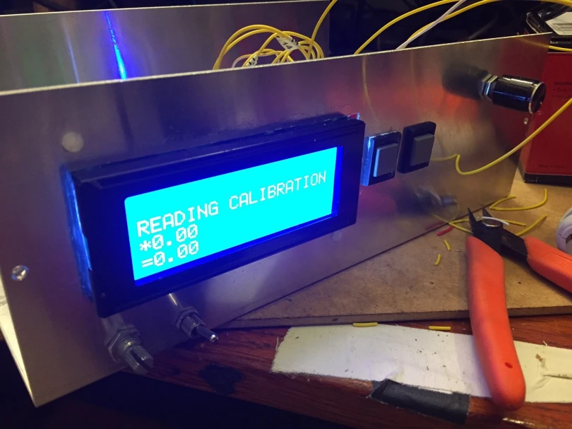
As I alluded to in my March bench report, I’ve been working on packaging up my old SI5351 VFO that sat on a breadboard for two years into a functional signal generator for the bench. That project is now essentially complete, though there are a couple of planned improvements in the works.

IMG_2249

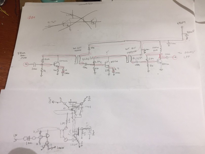
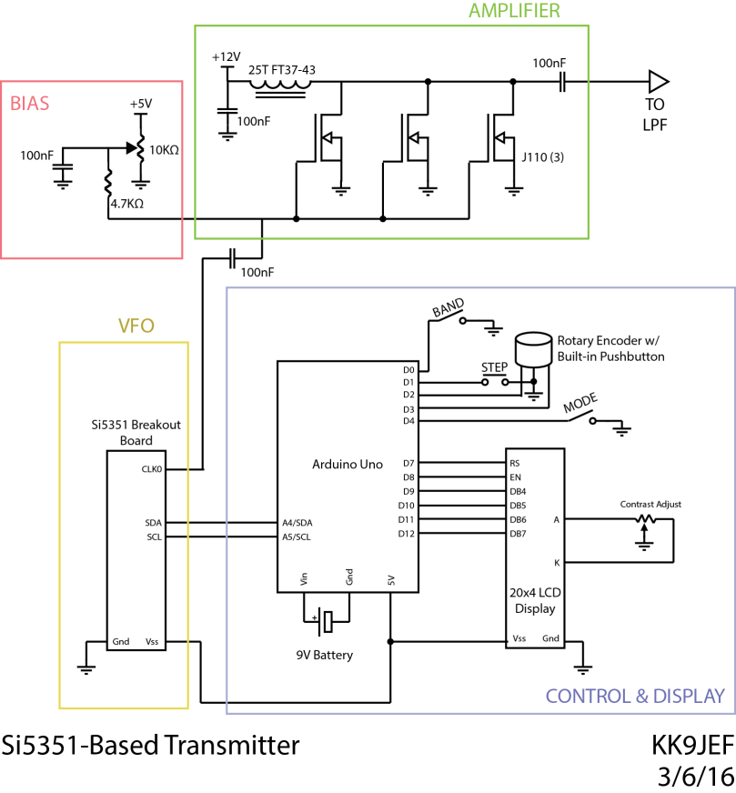
The heart of this project is a Silicon Labs Si5351 clock-generator IC, on a little interface module from Adafruit.  With an I2C interface, it can output square-wave signals at roughly 6dBm anywhere from 8Khz to 160 MHz. This nifty little chip has been around for a few years, and has been used in many a homebrew radio rig, including the work of N6QW, N2CQR, M0XPD, and other. Jason NT7S was essentially in building some of the earlier Arduino-friendly libraries for controlling the Si5351. With such a wide frequency range and the confidence that comes from XTAL-derived, PLL frequency generation, this little chip has breathed life into rigs both new and old.

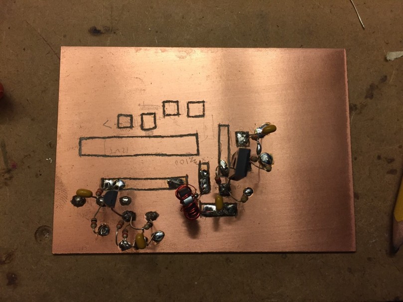
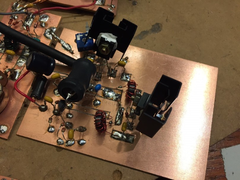
With the hardest part of building a SigGen (actually producing the darn frequency) neatly packed away in silicon, what remains for a builder is to wrap the thing in packaging to promote ease of use and flexibility. That’s where the fun of this project lay. The parts list ended up like so:

The project box and the LCD display were the most expensive parts of this build by a wide margin, although both would be available for quite a bit less with a longer lead time from oversees.

The SigGen has 4 different software modes:

  • VFO – The primary output frequency matched the displayed frequency. Frequency steps are 10kHz, 1kHz, 100Hz, and 10Hz.
  • Test – Same as VFO, but steps are 10MHz, 5 MHz, 1 MHz, 500kHz, 100kHz, 10kHz, 1kHz, 100Hz, 10Hz, and 1Hz.
  • Polyakov – Primary output frequency is half of the displayed frequency, for experimenting with half-frequency-driven mixers. Step size is the same as VFO mode.
  • BFO – Adjusts the secondary output frequency, for using the SigGen to drive a Superhet directly. Steps are the same as in Test mode.

The SigGen’s three pushbuttons (one built into the rotary encoder and two next to the LCD screen) do essentially the same thing in each mode:

  • Encoder: Changes the frequency step size, per the step options above.
  • Mode: Changes through the software modes, per above.
  • Band: Advances to the next highest Amateur band frequency, to aid with band-changes especially in VFO mode. For example, if the current frequency is 5.72MHz, pressing the Band button sets the frequency to 7.0Mhz, the bottom of the 40m band.

There are still a couple improvements I’d like to make, namely replacing the cheapo detent-based rotary encoder with a nice smooth continuous one, which can be had for about $10 on eBay – using a detent-based encoder as a VFO is a pain in the patoot. I’d also like to implement a sweep functionality to sweep through various filters, but that would require a bit more UI work as well.

This gadget has been complete on my bench for a month of so, and has already been useful in working on my variable-bandwidth superhet… but that’s a story for another post.

Hear you on the air!

73


Bench Report – HamRadio360 Podcast, Beach-40, SigGen, Power Meter Projects

A few weeks, back, I spent about half an hour chatting with Jeremy, KF7IJZ, for a listener-projects segment on the HamRadio360 Workbench podcast. That episode just went live this morning, if you want to take a listen online. Jeremy and I had a swell time chatting about the QST 40-9er Transceiver project I built awhile back, and ended up packaging with a laser-cut faceplate.

Seeing the podcast pop up got me thinking – from the last few months of posts, you’d think that I’d been spending all my time operating and that my bench was empty. Not so! There are three major projects milling about the bench these days. None are complete enough to merit a full post, but consolidating them all in to one post feels right.


First on the bench is the continuation of my Beach 40 Transceiver project, that I’ve been working on since the Fall. I’ve been making steady progress recently on the penultimate stage, the RF amplifier, which will take the ~10dBm modulated voice signal from the balanced modulator and turn it into ~33dBm (2W) of RF output power to send to the LPF and out into the world. The amplifier is a three-stage design, with a 2n3904 buffer feeding a BD139 driver and another BD139 final.

IMG_2291.JPG
Beach40 PA Schematic and Layout, in Graphite-O-Vision.

The module is assembled manhattan-style on single-sided copper glad, just like the rest of the project. The layout surrounds the +12V-on-transmit bus down the center of the PCB… more on that error later.

IMG_2155.JPG
The Beach40 PA mid-assembly – you can see the +12VT buss running down the middle, and the buffer and driver stages starting to take shape.

The module assembly and testing went fairly smoothly – using a variable-voltage power supply, it’s easy to vary the output power of the amplifier, and to observe the changes in PA heating that this causes. You can see the two large screw-on heat sinks on the BD139’s in the following pictures, as well as the the large ferrite bead which feeds the Final. There’s also a chunky 100uF cap at the DC input to the board for additional decoupling.

IMG_2288.JPG
The assembled Beach40 PA.


The problem I’m having now is the same one that plagued me way back in my assembly of the Virgin Receiver, my first first homebrew receiver: this amplifier would really love to be an oscillator. With the PA voltage set at 12V, any time the signal imput is sufficiently strong, the PA will fall hard into oscillation, and won’t stop until the PA voltage is brought way down or cut. I’ve been experimenting with emitter degeneration for the final BD139 (the original schematic has the emitter directly grounded). That’s helped, but not much. I’ve also changed the RF-carrying wires from hookup wire to coax, to mitigate feedback through other modules. Another help, but so far, the oscillation problem is still there. The next step will be to move the modules themselves around, to limit the amount that the high-power RF coming from the PA has to pass by earlier stages of the transmit chain (VFO, mic amp, balanced modulator) to try to eliminate feedback that way. Fingers crossed!


Next on the bench is a repackaging of an old project – my SI5351-based “VFO,” which for the better part of a year has been serving as my primary signal generator for experimental projects, spread out in all its Al-Fresco glory on a breadboard. With the amount of troubleshooting I’ve been going through on the Beach 40 project, I’ve decided to finally box up the SI5351, Arduino, and display into a proper project box, and make the thing a real SI5351-based Signal Generator. The schematic is essentially unchanged (minus the PA) since I used the project in my SI5351-based transmitter project, which is reproduced below:

CW Transmitter sCHEMATIC

To that end, I purchased an inexpensive nibbling tool and an expensive project box from the local Fry’s electronics, and have been working in the past couple weeks to marry the spread-out guts of the previous project with the clean lines of the enclosure. Biting out the large hole for the display 1/8″ at a time was time-consuming and strangely soothing.

At this point, the display and Arduino are connected, but I have yet to wire the two control buttons, rotary encoder, and Si5351 breakout board back into the Arduino. I also need a provision for getting the signal out the front of the darn thing, so I’m waiting on a shipment of SMA connectors and a jumper to go from the SI5351 breakout board to the front panel. So far, so good.

The code for this project is still on Github.


The last project on the bench is an RF power meter circuit, based on a circuit by W7ZOI from 2001. While the old scope-probe-across-a-50-ohm-load technique has proven very useful, I’ve found myself wanting a way to more reliably measure RF power at low levels, and to do it in a way that could be interfaced to a microcontroller or computer. To that end, I plan on using the W7ZOI circuit connected to an Arduino, much like Vu2ESE’s Sweeperino, to make digital power measurements.

IMG_2292.JPG

I rolled a little PCB for this project from OSHPark, and since that service provides PCBs in multiples of 3, I figure I’ll connect one board to an analog meter (for that old-school feel), one to an independent Arduino (for digital measurements), and embed one inside the SigGen project, for marrying signal generator and power measurement at specific frequencies. This last project, I figure, will be especially useful for examining filter behavior at HF and piping the information to a PC for display an analysis.


So that’s what’s on the bench at the end of March 2017. All of these will hopefully merit full posts in future as the projects come to fruition, but for now, the is the smorgasbord that is my bench.

Hear you on the air!

73

Beach 40 Build – Part 1: VFO

This post is part of a series: Building the VK3YE Beach 40 DSB Transceiver.

After listening some of of the recent episodes of the Soldersmoke podcast, and hearing about their adventures great and small having to do with VU2ESE’s BITX SSB transceiver, I’ve got a hankering to build something from scratch. Rather than jump in at the deep end, as it were, with an SSB transceiver, I’m starting with something more approachable: Peter Parker VK3YE’s “Beach 40” Double Sideband transceiver.

There’s a host of information on the internet about this project, but Peter’s project page, linked above, is a good place to start. You can also find some expanded notes on the build in a write-up of the Beach 40 Lo-Key magazine at the time, several years back.

The project is conceptually simple: A balanced diode ring mixer functions as the product detector on receive, and as the balanced modulator on transmit. Hook up the RF-pre-amp and an LM-386 audio amp, it’s a receiver. Hook up a mic amplifier and an RF power chain, it’s a transmitter. No muss no fuss. A handful of transistors, one IC, about 2-3W RF output.


Peter’s original design used a ceramic resonator in the VXO, though later versions of his employed a “super-VXO,” in which two or more similar crystals are paralleled for extra pulling range. I decided to use a true LC VFO in mine, as I’d like to cover from 7.125 to 7.300, the entire USA SSB range, if I can.

This is VFO design I started with. It’s a Hartley oscillator straight out of EMRFD. To that, I added a simple common collector buffer stage:

Beach 40 Schematics-01

Unfortunately, this design didn’t produce a high enough power level to drive a diode-ring mixer. Traditional diode ring mixers want to be driver with around +7dBm available power on their LO port, and I was only seeing 2 dBm. So I added an additional common emitter power stage to boost the signal level.

Beach 40 Schematics-02

Once the thing was oscillating at the proper power level, I spent a good hour tweaking the inductors and capacitors in the oscillator’s tank circuit to get the frequency spread down to the appropriate range in the 40m band. The final result is actually a bit wider than I’d like it to be, so some additional tweaking in the future will be necessary. I also found that, as I added additional shunt capacitance to the tank, I had to increase the coupling capacitor (originally 47pF, now 220pF), to get the circuit to continue to oscillate reliably. Here’s what I finally ended up with:

Beach 40 Schematics-03

One thing this process really drove home is the importance of shielding the VFO – the hand capacitance effects alone during debugging were making me a bit crazy. Sometimes just reaching in to hook up a scope probe would cause the thing to stop oscillating or start oscillating, or develop some parasitic oscillation…. woof. I’ll have to build a little box for the thing now that it’s essentially in the right shape. But for the moment, here it is, in all is little glory:

IMG_1226

As I’ve documented before, I find that a variation on the Island Squares method of circuit construction is very approachable for this kind of circuit building. Essentially, small isolated pads are cut into a piece of copper-clad board using a dremel, and the components soldered to those. Ground connections attach to the ground plane of the board. It’s easy and quick, and allows for long connections to be made when necessary (the 12V bus on this project spans one whole side of the board, with de-coupling along the way).

IMG_1222

I’m planning to build the next stages in the order Peter suggests in his Lo-Key article: Audio output amplifier, the diode-ring mixer, low-pass filter, mic amplifier, and the RF power chain. Since he originally published the design, Peter’s changed from a discrete-component to an LM386 audio amp, added an RF pre-amp, and stuck an L-Match tuner inside the case as well. I’m planning on adding the first two modifications, and perhaps an outboard unit for the third.

Hear you on the Air!

73

Giving the Virgin Some Mobility

As wonderful as it was to ‘complete’ the Virgin Receiver and have a set of ears to start listening on, more and more I find myself wishing for the ability to change frequency and explore the 40m band a bit. To that end, I’ve been experimenting with hooking my Si5351-Based VFO directly to the Virgin as an easy way of giving it the ability to QSY.

(The VFO, as it happens, has a few more features nowadays, including being able to act as  WSPR beacon and having an auto-CQ mode. The code, as always, is on Github.)

Here’s the receiver as built:

schemeit-project(1)

Jason NT7S dropped a hint in one of his older blog posts that the Ne602 likes to see about 300 mV p-p when being driven externally, and that a 10dB pad could be used to bring the Si5351 down to this level. To that end, I put together a quick Pi-attenuator consisting of one 120-Ohm and two 150-ohm resistors.

IMG_0549
A tiny 10dB pi-attenuator.

The attenuator plugs directly into the receiver where the crystal X1 usually sits, in a little 1×3 piece of female header. The output of the 10dB pad plugs into the side of the header that’s connected directly to pin 6 on the NE602; the ground on the attenuator plugs into the other side of the header, and is therefore connector to ground on the receiver.

The longer red and white wires you can see attached to the pad connect to ground and the CLK0 output of the Si5351. Here’s the current setup, spread out on the bench.

IMG_0546

It’s already quite successful! I can scan up and down the 40m band and pick out CW signals pretty well. SSB signals are faint and pretty un-hearable. Unfortunately, for some reason, my receiver has also turned into an AM radio:

I think some kind of high-pass filter is in order here. There’s always been a bit of AM bleedthrough with this receiver, but given that the AM stations are attenuated by the RF Pot on the receiver, it seems like most of this signal is coming in through the antenna and not, say, bleeding into the audio amp.

Hear you (all around the band) on the air!

73


Si5331-Driven Transmitter – Beginnings

In Spring, a young man’s fancy turns to thoughts of transmitters. Having recently completed a receiver, and with the weather starting to warm a bit, I’ve got an itch to actually get on the air and talk back to the stations whose code I can now (slowly, painfully) decode.

Re-purposing some hardware and code from my DDS VFO project, I’ve been working on on a digitally controlled CW transmitter based around an Si5351. This is by no means an original thought, and my designs are largely based on Qrp-Labs’ Ultimate3s Kit. You can check out that original design over on the QRP-Labs site, under the PCB assembly instructions.

Essentially, this transmitter uses an Si5351 DDS clock chip to directly synthesize the desired output frequency, at up to 200 Mhz. This frequency is then amplified by a simple FET amplifier to approximately a 1W output level, then passed through a low-pass filter and out to an antenna. The Si5351 is controlled over i2c by an Arduino Uno, which has an attached LCD, a rotary encoder, and a couple buttons for frequency and band control. The updated code for this project is on Github.

Here’s a block diagram of the transmitter:

Si5351TransBck-3-6(3).png

The nice thing about this design is that the main frequency-dependent component is the low-pass filter; the Si5351 should be stable enough for CW contacts up to at least 50MHz. (Without an ovenized environment for the reference clock or some GPS disciplining or similar, there’s still a little drift and inaccuracy, but I don’t think it will be noticeable.) Above HF, I’d expect to see diminishing returns from the FET amplifier. But switching HF bands should just mean switching LPF filters and pressing a button on the VFO.

Here’s the circuit as constructed, up to where the LPF would go:

CW Transmitter sCHEMATIC
The simple Si5351-based transmitter, with a 3-FET amplifier.
Let’s walk through the circuit starting from the signal generator and working out toward the antenna. The output of CLK0 on the Si5351 is coupled into the amplifier with a 100nF cap. This drives the gates of three J110 FETs, and is biased upward by a voltage divider formed by a 10K pot and a 4.7kOhm resistor between 5V and ground. The power end of this voltage divider is bypassed to ground with a 100nF cap.

Power for the amplifier is fed from a nominal 12V (or lower) through an RF choke, in this case 25T on an FT37-43, into the FET drains. A 100nF cap here helps further bypass RF to ground at this point. Output is taken off the drains through a final 100nF cap. The FET sources are grounded.

While an actual RF transistor like a BS170 would likely be ideal, I had a bunch of J110 FETs in my bin after my last trip to California, so that’s what I used. They’re only rated for about 300mW dissipated power, so I’ll need to be careful with my heat sinks and duty cycle until I can replace them with something a little more sturdy.

IMG_0393
Three J110 FETs with their heat sinks on a piece of copper clad. In the back you can see the PA power coming in through the black alligator clip via the small RFC. The bias pot is on the left, signal comes in on the red wire on the bottom, RF out via the BNC connector on the right. The big white box down in the bottom is a 51 Ohm, 5W resistor I was using as a basic dummy load for testing
Preliminary results are encouraging – I hooked the output of the above circuit directly to a dummy load with no low-pass filter and ran the clock generator at 7.050MHz. I assessed power by reading off the peak voltage on an oscilloscope.I started with just 1 J110 and a 5V PA supply instead of 12V. This yielded about 9V peak-to-peak, or 200mW into 50 ohms. Installing the other two J110s bumped the output up to 10V P-P, or 250mW. Finally, after installing heat sinks on the FETs for safety and taking the supply voltage directly from a 12V SLA battery (~13.2V), the output hit 22V P-P, or 1.2W into 50 Ohms.   This last reading was verified with the power meter on an MFJ versa tuner.

IMG_0376
The transmitter spread out on the bench, with the display and Arduino at the top, the amplifier visible on the copper-clad in the middle, and a bulky MFJ tuner at the bottom acting as dummy-load and power-meter.Power provided by the 7Ah, 12V SLA battery at top-right.
I’ll need to put a little elbow grease into low pass filters before putting this on the air, because even on a scope the signal looks a bit gnarly. But first the first time, I’m responsible for 1W of Homebrew RF power. Watch out!

73


Si5351 DDS

Update: for more information on the evolution of this project, see First Steps in Arduino Driven DDS and Si5351-Driven Transmitter.

I’ve ordered a breakout board for Silicon Labs DDS chip, the Si5351, as a starting point for working with signals and forming a homebrew VFO. I think the first thing I’d like to try is putting together a “Polyakov-Style” direct-conversion receiver using KE3IJ’s excellent descriptions, probably for the 40m band, as a place to start. I’ve already got the bulk of the parts in my junk-bin, and a couple toroids are on their way

The folks at Etherkit have put together a very full featured library for the Si5351; I just wish it wasn’t so big! It eats up about 3/4 of the space on an Atmega328 by itself, which doesn’t leave a whole lot of room for other programming. Maybe it’ll be worth me implementing i2c of the Si5351 directly, since I don’t think I’ll be using a lot of the features of the Si5351 Etherkit library to start with.